Nanofabrication Research Faculty
Suryakanthi (Surya) Srinivas Rachamadugu
Observational Cosmology Laboratory (665)
Tell us about the research projects you’re currently working on.
Micro-Electro-Mechanical Systems (MEMS) are tiny devices (about a millionth of a meter in size) that combine electronic and mechanical components. They essentially act like miniature moving machines. I’m working on developing a MEMS device that enables Multi-Object Spectroscopy (MOS), a technique that lets an observatory collect spectra from many targets at the same time and dramatically improves the efficiency with which the observatory can gather astronomical data. Specifically, I work on the next generation of Microshutter Arrays (MSAs). These are silicon-based MEMS made up of thousands of tiny shutters, and they are currently one of the most robust and effective ways to carry out MOS in space. MSAs make large-scale data collection for space telescopes far more efficient. The first generation MSA was deployed on the James Webb Space Telescope (JWST), and that MSA has been instrumental in enabling multi-object spectroscopy in JWST’s Near Infra-Red Spectroscope (NIRSpec) instrument.
I’m working on developing Next Generation Microshutter Arrays (NGMSA) for a series of sounding rocket missions called Far-ultraviolet Off Rowland circle Telescope Imaging and Spectroscopy (FORTIS) sounding rocket missions, which aims to observe globular clusters in the Milky Way galaxy. I’m also working on the fabrication and characterization of a Large Format (Microshutter) Array (LFA) that will eventually be deployed in the Habitable Worlds Observatory (HWO) mission. This LFA could help us realize multi-object spectroscopy in the ultraviolet-visible range in the upcoming planned HWO mission.
Another project I’m involved with is the Miniature Electron Probe for In Situ Elemental Microanalysis (MiniEPMA) instrument, which aims to develop a lightweight and low-power electron probe microanalysis space instrument using a carbon nanotube-based electron source at its core. This means that the MiniEPMA can efficiently generate high-energy electrons, which on interaction with an extra-terrestrial surface induce X-ray emission from the surface. By analyzing these emitted X-rays, MiniEPMA can produce a spatially resolved map of the surface’s elemental composition. It can detect both light (lighter than sodium) and heavy elements, which is a key feature that makes the instrument novel. Such an instrument would provide an in-situ way of performing spatially resolved elemental analysis of surfaces in extra-terrestrial regions.
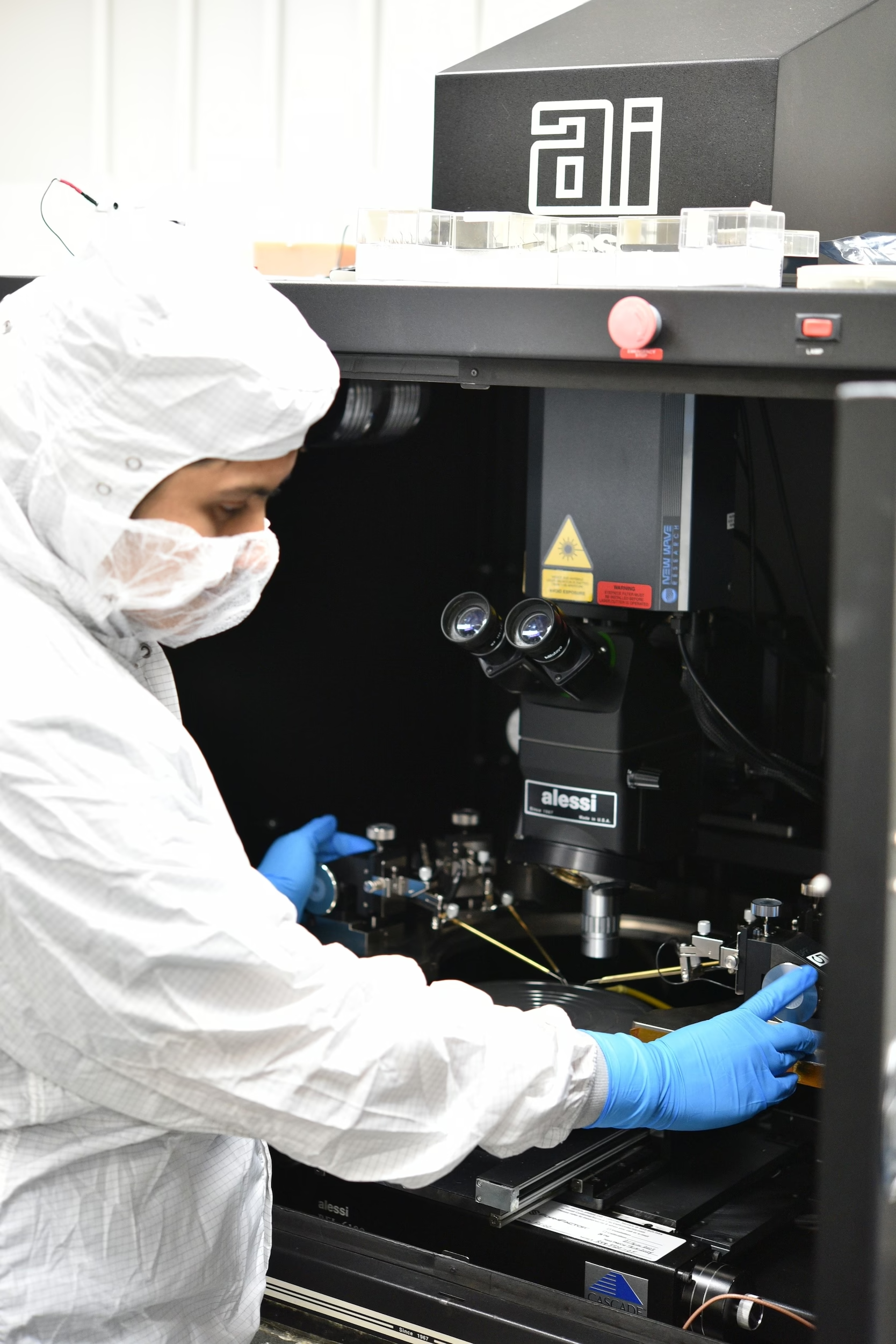
I’ve worked on developing electronics for characterizing the NGMSA and the Carbon Nanotubes based Emitter Arrays on these projects, as well as helping with collecting data on how well they have been fabricated and how well they perform. I also work on packaging these devices to ensure that the micron-sized components can reliably communicate with the much larger electronics that drive them.
Did you always know you wanted to work with nano-scale systems?
Not always! As an undergraduate student, I just knew that I found the courses that touched on physics at the nanoscale (where quantum phenomena become significant) very interesting. I was fascinated by the various exotic phenomena possible with systems that are small enough for quantum effects to influence their behavior. I worked with graphene-based Field Effect Transistors (FETs), where a few layers of carbon atoms (graphene) form a conductive channel, whose properties can be tuned by an electric field. I also studied twisted graphene devices, where two graphene layers are slightly rotated relative to each other. Around a certain “magic” angle of rotation between these two graphene layers, the electronic bands flatten out and lead to counter-intuitive behavior. It was while I was working with these devices that I learned about phenomena that various people had coaxed out of the system such as the quantum hall effect and superconductivity – this was the experience that made me realize I want to work on nanoscale systems!
If you could broaden your research, what would you work on?
I am deeply interested in nanoscale and condensed-matter physics, and if I were to broaden my research, I would like to develop physics-based simulation tools to guide fabrication experiments for nanoscale devices such as the micro shutters and MiniEPMA components I currently work with. These systems often exhibit behaviors whose origin is difficult to elucidate experimentally, and fabrication cycles can be slow and resource intensive. I wonder if it would be possible to build high-fidelity simulations based on the underlying physics of these devices, which can then be calibrated with empirical data and provide deeper insight into their behavior. Once validated, these models could direct the design of subsequent fabrication experiments, enabling a more targeted and efficient exploration of nanoscale phenomena while remaining firmly rooted in hands-on investigation.
I am also interested in developing simplified models that capture the electrical behavior of complex nanoscale and MEMS devices. Through my work on microshutters, I have seen how valuable accurate electrical representation of components could be for system integration, as they provide engineers with clear data on a component’s characteristics. Creating equivalent circuit models could broaden the impact and usability of the nanoscale technologies I study by making device behavior more accessible and easier to integrate into different system designs.

Who or what inspires you?
One of the images that has always captured my imagination is the image of the Pillars of Creation (captured by the Hubble Space Telescope) that I saw in space magazines as a child. It was exciting to see a higher-resolution version of the same image taken with JWST, released around the time I got a college degree. I’m amazed that I’m now working on MSAs, a core component of JWST, and helping adapt it for the requirements of HWO. The knowledge that I’m building on something deployed in JWST, which produced the highest resolution image we have of the Pillars of Creation, inspires me a lot.
I’m also inspired by visionaries like James Maxwell and Ludwig Boltzmann. They simplified diverse concepts into elegant frameworks, recognized their broad applicability and developed well used general theory. Another inspiring visionary would be Thomas Young, because his experiment on the wave nature of light opened a can of worms that changed our understanding of literally everything!
Closer to home, I’m inspired by the people I work with at Goddard, who approach every challenge with curiosity, adaptability, and resilience. My friends and family also motivate me through their enthusiasm for my work and their unwavering positivity and support.

What space mission are you most excited about?
One of the missions I’m the most excited about is the Habitable Worlds Observatory, as it is the next great observatory to be launched by NASA and will be a successor to the Hubble Space Telescope. This telescope is planned to have ultraviolet, infrared and visible light spectrographs. It will use improved versions of technologies deployed in JWST and the Roman Space Telescope, including multi-object spectroscopy, picometer level spacecraft stabilization and coronagraphy. With these technologies, HWO is poised to answer the question of whether there are other habitable worlds apart from Earth.
This is really exciting because I think we’ve all wondered if it is possible that life as we know it exists outside of Earth, and it would be amazing to have extensive data to answer this question. Apart from this, HWO will also study a wide range of topics related to galaxy evolution!

What do you enjoy most about your job?
Every day at my work here at NASA, I’m empowered to ask questions and propose the problems I’d like to explore. I also get to continually learn, fabricate and test electronics and MEMS/nanoscale, which I have been enjoying a lot!
Another part of my job I particularly enjoy is collaborating with colleagues who bring deep expertise and enthusiasm to their work. Their insights challenge me to think more broadly and help me strengthen my own approach to problem solving. Their support enables me to become a better engineer and researcher. I’ll forever be grateful to the people I’ve worked with here, and they’ll stand out as mentors to me for the rest of my career.
What is one of your favorite moments in your career so far?
One of the most memorable moments in my career was learning that the NGMSA module I helped package had flown on the Off Axis (OAx) FORTIS sounding rocket mission and successfully produced the first-ever ultraviolet multi-object spectrum! The 2024 FORTIS mission, carried out by our collaborators at Johns Hopkins University, launched from White Sands, New Mexico, in August 2024 and successfully observed the globular cluster M10 in the Milky Way.
(Read More: OAxFORTIS Sounding Rocket Mission Successfully Completed)
Published Date: .
Hometown:
Hyderabad, India
Undergraduate Degree:
Bachelor’s in Electrical and Communications Engineering, BITS Pilani, Goa, India
Post-graduate Degree:
Master’s in Electrical Engineering, University of Virginia, Charlottesville, VA